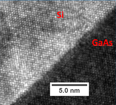
| 
              
                
                  | Sponsors Messages |  
                  | ALTEC
                    EquipmentModular EpiCentre Deposition Stage for MBE applications:
                    the EC-I series is the latest model in the very successful
                    range of EpiCentre stages, providing state-of-the-art
                    performance for various growth and deposition techniques
                    including MBE, sputtering and CVD... [More]
 |  
                  | IrconIrcon extends Modline 7 series by two new infrared
                    thermometers and a new processor box. The new 7V line has
                    been especially designed for the semiconductor industry,
                    while the 75 series now comprises a new high temperature
                    model dedicated to heat treating and annealing... [More]
 |  
                  | RiberRiber has launched the new Compact 21 Discover 3-inch
                    substrate MBE research system. The entire vacuum hardware
                    of the Compact 21 Discover is conveniently presented in a
                    fully open way to permit a unique 360° access to the
                    system for easy cell filling, maintenance and new
                    accessory additions.... [More]
 |  
                  | Tescan
                        Orsay Holding TESCAN ORSAY HOLDING group develops SEM and DualBeam for
                      semiconductor applications, in particular:
 
                        [More]MAIA and GAIA: FEG SEM and DualBeam based on an
                          immersion electronic column (for higher resolution at
                          low voltage)New GM large chamber with stage able to accommodate
                          12" wafersNew softwares dedicated to semiconductorsNew accessories included into the SEM (FIB): AFM ,
                          TOF -SIMS , laser interferometer stage... |  | 
 | 
              
                
                  | Recently Published |  
                  | 
                      
                        
                          |  
 | 
                            Formation of Monocrystalline Silicon-Based Mie
                            Resonators via Silicon-on-Insulator DewettingM. Abbarchi et al.
 We report the capabilities of a dewetting-based
                            process, independent of the sample size, to
                            fabricate Si-based resonators over large scales
                            starting from commercial silicon-on-insulator
                            (SOI) substrates... [More]
 |  
                      
                        
                          |  
 | 
                            Selective area epitaxy of InAs/AlGaSb tunnel
                            diodesL. Desplanque et al.
 In this study, selective area (SA) growth of InAs
                            by molecular beam epitaxy (MBE) is used to define
                            small area near broken gap AlGaSb/InAs tunnel
                            diodes grown on a GaSb:p+ (001) substrate... [More]
 |  
                      
                        
                          |  
 | 
                            LEEM study of the dynamics of solid state
                            dewettingF. Leroy, F. Cheynis, P. Muller
 Using low-energy electron microscopy (LEEM), we
                            have studied, in-situ and in real time, the
                            dewetting of Si(001) and Ge(001) thin films on
                            amorphous silicon dioxide substrates... [More]
 |  
                      
                        
                          |  
 | 
                            Low Temperature Epitaxy in a Plasma Enhanced
                            Chemical Vapor Deposition environmentLPICM
 Can we grow epitaxial silicon films at low
                            temperature (~200 °C) in a PECVD environment? the
                            most common answer is: no. Still, this is what
                            researchers at LPICM have been convincingly doing
                            over the past years... [More]
 |  
                      
                        
                          |  
 | 
                            High quality (11-22) semipolar GaN nearly free
                            of basal stacking faults grown on 2 in.
                            patterned sapphire substrate by MOCVDF. Tendille et al.
 High quality semipolar (11-22) GaN layers have
                            been achieved by MOCVD on 2 -in. sapphire wafers
                            by performing the selective area growth of GaN
                            nitride from the inclined c-facets of a patterned
                            sapphire substrate (PSS)... [More]
 |  
 
 |  
              
                
                  | Of Interest for the Epitaxy Community |  
                  | Joint
                    laboratory Annealsys and Institut des Nanotechnologies
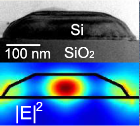
                    de Lyon for CVD/ALD process developmentAnnealsys is pleased to announce the creation of a
                    joint laboratory (InCVD) with Institut des
                    Nanotechnologies de Lyon (INL - UMR CNRS 5270) supported
                    by the French National Research Agency (ANR: Agence
                    Nationale de la Recherche). The InCVD laboratory is
                    dedicated to innovating chemical vapor deposition
                    processes and associated materials and will be directed by
                    Dr Catherine Dubourdieu (INL) in association with Dr
                    Jean-Manuel Decams (Annealsys)... [More]
 
 New epitaxy
                      equipment at NanoTecMat technological platform
 A silicon-germanium MBE equipment (SG800 from DCA
                    Instruments) was recently installed at NanoTecMat
                    technological platform. This MBE chamber is designed for
                    200mm wafer size. It is connected to a cluster tool type
                    UHV central distribution chamber allowing future expansion
                    with additional growth chambers, analysis chambers or
                    other processing chambers... [More]
 |  


                  | Upcoming Events |  
                  |  28
                    th SYMPOSIUM ON SURFACE SCIENCE 2015Sunday, March 22 - Saturday, March 28, 2015
 Les Arcs 1800, Bourg Saint Maurice, France
 Organizers: P. Muller, G. Renaud, F. Leroy, F. Cheynis and
                  S. Curiotto
 All information and online-registration is provided on the
                  web page: http://www.cinam.univ-mrs.fr/3s15
 |  


                  | Job Opportunities / Research |  
                  | Postdoctoral
                    Position - CINaMThis proposal for a post-doc position is supported by the
                    French Agency for Research.
 The main goal of our project is to develop a basic
                    understanding of the statics and dynamics of
                    solid-solid-vacuum triple lines via a study of the
                    dynamics of dewetting of a thin film. More precisely we
                    want to tackle two problems (i) the influence of chemical
                    reactivity at the triple line and (ii) the role of
                    substrate heterogeneity (topographical or chemical) on the
                  triple line behaviour... [More]
 Title: Triple-line
                    dynamics and solid-state dewetting
 Keywords:
                    Dewetting, Thin films, LEEM, Atomic probes
 Duration: 18 mois
 Laboratory: CINaM,
                    UMR CNRS, Marseille, France
 Contact: muller@cinam.univ-mrs.fr
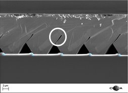
 |  
 
 |