Soutenance de thèse - Hadjer Ouaddah - Mardi 14 Décembre 2021 - Study of crystalline defects issued from silicon solidification. Effect of impurities and correlation between crystallography, physicochemical and electrical properties.
Annonce de soutenance de thèse
Madame Hadjer OUADDAH
(ED n°352 : Physique et sciences de la matière)
soutiendra publiquement ses travaux de thèse intitulés :
Study of crystalline defects issued from silicon solidification. Effect of impurities and
correlation between crystallography, physicochemical and electrical properties.
dirigés par Madame Nathalie Mangelinck-Noël (Département MATER, Equipe MCA) et
Madame Isabelle Périchaud (Département DETECT, Equipe IRM-PV)
le mardi 14 décembre 2021 à 9h30
Salle des thèses, Campus de Saint Jérôme
et en visioconférence
Participer à la réunion Zoom
https://univ-amu-fr.zoom.us/j/95731678359?
pwd=QUk1cjl4RDFOVGZuNWtZUkJjTDl0dz09
ID de réunion : 957 3167 8359
Code secret : 483394
Summary
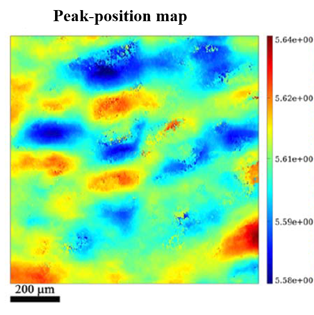
An experimental approach including several techniques was used to characterize structural defects issued from the solidification by in situ X-ray imaging during solidification and by complementary ex situ techniques to characterize and quantify the grain structure, crystalline quality, and deformation. The composition and segregation of impurities were measured in correlation with the defect characterization and correlated to minority carrier lifetime measurements. The analysis shows significant influence of light impurities and metallic impurities on Si solidification and on the electrical properties. In the presence of light impurities, a higher frequency of grain nucleation is observed, it is linked to the presence of precipitates. The resulting grain structure is constituted by a higher proportion of high order twin and of random angle grain boundaries compared to the case of low contaminated samples. Moreover, local deformations are induced by the presence of SiC and are at the origin of SABGs (Small Angle Grain Boundaries) formation. The electrical properties are degraded (lower and inhomogeneous minority carrier lifetime) in the presence of light impurities compared to the case of pure Si materials. In Cu contaminated samples, no significant effect on the grain structure was evidenced. However, coherent Σ3 twin boundaries, which are defects of high crystalline quality, can be active in presence of Cu. This observation was correlated to Cu segregation at the level of these grain boundaries. During this study, recent progress concerning the in situ characterization of the defect formation dynamics during solidification allowed to open new prospects.
Key words: Silicon, solidification, in situ characterization, structural defects, impurities, electrical properties.
Composition du jury
Anne Kaminski - Cachopo Rapporteure Université Grenoble, France
Kozo Fujiwara Rapporteur Université Tohoku, Japon
Stéphanie Escoubas Examinatrice Aix-Marseille Université, France
Guy chichignoud Examinateur CNRS
Nathalie Mangelinck-Noël Directrice de thèse CNRS
Isabelle Périchaud Co-directrice de thèse Aix- Marseille Université, France