Séminaire - 30/05/2022 - Thierry Duffar - DEFECT ENGINEERING IN BULK CRYSTAL GROWTH
Invitation : Nathalie Mangelinck-Noël (Eq. MCA, Dep. MATER)
Diffusion : IM2NP, CiNaM, Irphe, LP3, Madirel (via P. Boulet), PIIM (via T. Angot), CPT (T. Martin), Fédération de Chimie (via S. Viel)
SEMINAIRE Lundi 30 Mai 2022 à 11h
Salle des séminaires de l'Im2np, campus de Saint-Jérôme, 1er étage Bâtiment Poincaré
Thierry Duffar
Univ. Grenoble Alpes, CNRS, Grenoble INP, SIMAP, F-38000 Grenoble, France
DEFECT ENGINEERING IN BULK CRYSTAL GROWTH
Most bulk crystal growth processes, such as Czochralski, Bridgman, Verneuil, were invented more than one century ago. Fifty years later, crystals appeared to be key materials for advanced technologies: electronics, optics, sensors and so on. Consequently, these processes have been developed in order to reach industrial standards in terms of productivity, reliability and costs. Anyhow, placed on a very competitive market, companies are continuously facing the need of improving their growth technology in order to get larger, better and cheaper crystals.
Obviously, growth conditions directly control the crystal quality and it is of uppermost importance to understand the physical phenomena involved during the growth and how they affect the defect distribution inside the crystal. This is well known as far as individual, independent, defects are considered so that this basic knowledge can be used for any kind of crystal and growth process. In this respect, I will show how process charts can be drawn in order to quickly define the growth condition for producing a given crystal.
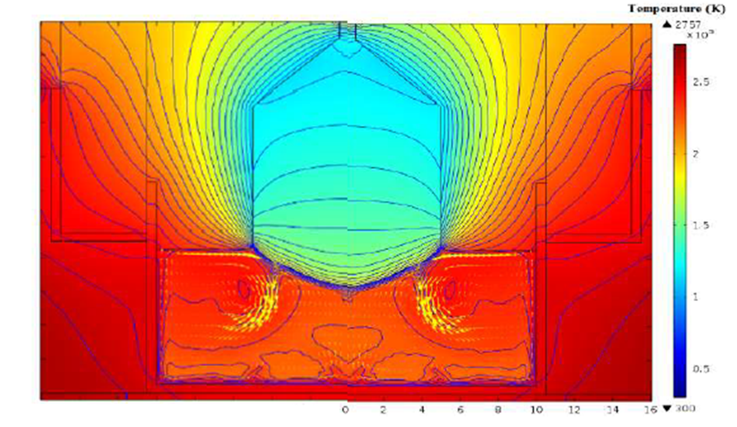
A further step forward concerns the precise design of the process for obtaining given crystals with a given quality. For this, the passed thirty years have seen several groups worldwide developing numerical models in order to investigate the details of the processes. This activity led to the offer of devoted numerical simulation software, which are now commercially available at the industrial level. I will show, on some examples, how numerical simulation can help solving real industrial crystal growth issues.
However, the situation becomes more complex when crystal defects cannot anymore be considered independently. In such situations, it will be shown, through some industrial examples, that an acceptable compromise between contradictory growth parameters is difficult to obtain. Numerical modelling of such complex coupling remains a challenge.