Séminaire - 13/07/2022 - Tihomir Knezevic - The versatility of boron layer deposition technology and its applications in semiconductor devices
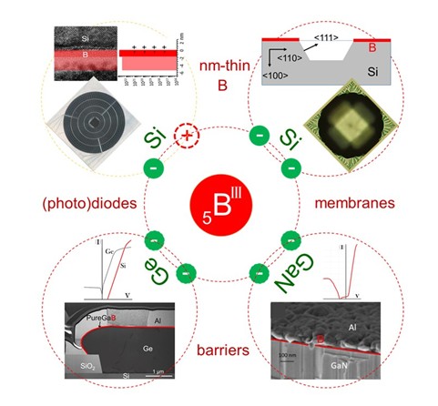
Technology for deposition of nanometer-thin boron layers (PureB technology) directly on silicon, germanium, and gallium-nitride substrates has shown great potential for advancing various semiconductor devices such as transistors, diodes, avalanche diodes for single-photon detection, low-energy electron detectors, and radiation detectors for wavelengths between X-ray and infrared part of the spectrum. The application of thin boron layers in semiconductor devices ensures favorable electrical and physical properties such as low dark currents, high stability, electrical and chemical robustness of the layers. Only several atomic layers of pure boron can achieve the suppression of the electron injection coming from the substrate with the same efficiency as with deep p+n junctions. The layer thickness of only a few nanometers does not affect the absorption of photons and low-energy electrons thus ensuring excellent sensitivity and optoelectrical performance. Boron layers can be deposited using different chemical and physical deposition methods at temperatures from 700 ° C to 50 ° C, which is why PureB technology is compatible with the CMOS process and has great industrial potential. From numerous experimental and theoretical analyses, it has been concluded that good electrical and optical characteristics are determined by the properties of the boron-semiconductor interface.