SEMINAIRE Mardi 5 Février 2019 à 11h00
Invitation : Sandrine BERNARDINI (Eq. MCI, Dep. DETECT)
Diffusion : IM2NP, CiNaM, Irphe, LP3, Madirel (via P. Boulet), PIIM (via T. Angot), CPT (T. Martin), Fédération de Chimie (via S. Viel)
SEMINAIRE Mardi 5 février 2019 à 11h
Salle des séminaires de l'Im2np, campus de Saint-Jérôme, aile 1, niveau 6 service 161
Luis Fernando da Silva
Center for the Development of Multifunctional Materials
Federal University of São Carlos - UFSCar
São Carlos SP - Brazil
Preparation of Nanostructures and their Application as UV-light assisted Gas Sensors
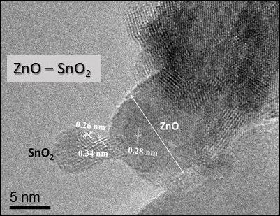
The investigation of metal oxide semiconductors (MOS) is a fundamental point in the area of physics, chemistry, and material science engineering, in particular nanostructured compounds. These materials have attracted attention due their unique physical and chemical properties, and especially its practical application in several areas, such as gas sensors, catalysis, solar cells, and hydrogen production. In the case of gas sensors, great effort has been devoted to the development of micro and/or nanodimension devices, facilitating its integration into an electronic circuit. Among the important gaseous species to be detected are NO2, CO, O3, and BTEX (benzene, toluene, ethylbenzene and xylene). In past decades, MOS are considered a fascinating class of materials in the area of science, especially to be applied as sensing layer. Among them, the wide-gap semiconductors (e.g. SnO2, ZnO, In2O3, and WO3) have been prepared by physical and chemical routes. Recently, the photoactivation process has been an efficient approach for the operation of gas sensors at room temperature, avoiding thus, the high-temperatures commonly used in the thermal activation of such devices. Nevertheless, the electronic effects adverse during the charge separation process, reduces the potential of the isolate semiconductors. Thus, the heterostructures combining two metal oxide semiconductors have been investigated as an alternative way to reduce the recombination processes. In this presentation, it will be presented the synthesis of nanostructures via microwave-assisted synthesis and their application as gas sensors operating at room temperature under UV-illumination.


