Séminaire 23/09/19 - David Martrou - Controlling the electric charge of gold nanoplatelets on an insulator by field emission nc-AFM
Invitation : Christian Loppacher (Département PHANO, Equipe Nano et Nano-MATMOL (IM2NP/CINaM).
Diffusion : IM2NP, CINaM, Irphe, LP3, Madirel (via P. Boulet), PIIM (via T. Angot), CPT (T. Martin), Fédération de Chimie (via S. Viel), CP2M
SEMINAIRE Lundi 23 septembre 2019 à 15h00
Salle des séminaires de l'Im2np, campus de Saint-Jérôme, aile 1, niveau 6 service 161
David Martrou
CEMES, GNS, Toulouse
Controlling the electric charge of gold nanoplatelets on an insulator by field emission nc-AFM
Flat metallic islands on an insulating substrate can be used as electrons reservoir to contact a molecule or a graphene nanoribbon in a planar geometry for molecular applications. Moreover, to allow the characterization by NC-AFM [1] of the molecule connected to the metallic nano-island, the insulating substrate should be atomically flat, and the nano-island should not have more than 3 monolayer thickness. We have chosen ten years ago to use the wide band gap semiconductor AlN (6.2 eV) as the insulating substrate. The optimization of the AlN growth by molecular beam epitaxy (MBE) was realized on 6H-SiC(0001) substrate with the (√3x√3)-R30° reconstruction obtained by progressive enrichment of Si atoms [2]. The RHEED and NC-AFM studies coupled to DFT and thermodynamic calculations allowed us to determine the atomic structure of the (2x2)-Nad reconstruction of the AlN layers grown at 10 nm/h [3]. To grow metallic nano-islands on the AlN layers, several metals have been used (Mg, In, Ag and Au) [4], and only the gold allows to obtain one monotamic height nano-ilands. Low temperature Qplus images of these gold nano-islands coupled to DFT calculations show that some gold atoms are chemically bonded to the Al and N atoms of the AlN (2x2)-Nad reconstruction [5].
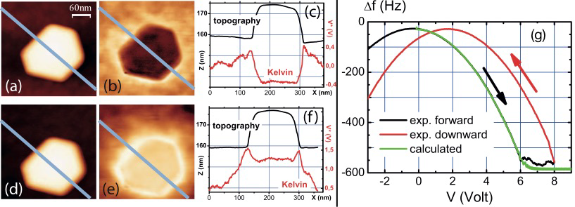
The challenge is then to stabilize the charge on these gold nano-islands for a time long enough to perform in-plane operations. The controlled charging one gold nano-island was realized using field emission from the the AFM tip. To understand the charge mechanism, we have reproduced this controlled charge on 2D Au nanocrystals deposited on a SiO2 insulating substrate. The charge state is characterized by Kelvin Probe Force Microscopy (KPFM) (see figure 1) [6,7]. Our results demonstrate that the charge of a metallic island on an insulating layer can be controlled by electron field emission to or from the tip of a nc-AFM by monitoring Δf(V) spectroscopy curves. The procedure works for both polarities, electrons being emitted by the tip or the substrate. As shown by an analytical model and complementary numerical simulations, the rise of the island's potential upon charging leads to a constant charging current and tip-island electric field [8]. Our measurements suggest that this method can be used to set the island's potential with a single-electron precision. This degree of control is achieved thanks to the increased stability and sensitivity provided by the UHV environment. The procedure is robust and opens the way to original experiments, such as establishing a bias at the extremities of a molecule connected between two islands or exploring locally the charge leaking mechanisms across an insulating layer.