
Equipe Nanostructuration (NANO)
Responsable d'équipe-s :
Laurent NONY
Responsable-adjoint-e-s :
Sylvain CLAIR
- Campus de Saint Jérôme, Marseille
Aile 1, niveau 5, Service 151
Salle des doctorants: 04.13.94.52.76
Salle IPE: 04.13.94.52.79
Salle AFM-STM: 04.13.94.52.45
- Campus ISEN Yncréa Méditerranée, Toulon
![]()
- The Nanostructuration Team is part of the inter-laboratory team Nano-Mat-Mol with CINaM laboratory.
- ISEN site in Toulon
Research Subjects:
- On-surface synthesis
- Electronic properties of organic/inorganic interfaces
- Molecules on wide-gap surfaces
- Surface Enhanced Raman spectroscopy and Near Field Optics
- Catalytic Scanning Probe Nanolithography (c-SPL)
- Press Releases:
- Research
On-surface synthesis is a newly developing field of research that aims at making use of well-defined solid surfaces as confinement templates to initiate chemical reactions. The concepts of supramolecular chemistry are here applied to provide well-defined functional surfaces from the “bottom-up” self-assembly of nanometer-sized elementary building-blocks. The interest for creating covalent nanoarchitectures directly on surfaces is manifold. On-surface synthesis gives access to original reactions mechanisms in mild conditions that would be not easily accessible in standard chemistry conditions. Also, it represents an efficient route to the formation of robust organic networks and 2D polymers. Finally, the full range of available surface science techniques can deliver exquisite characterization of the different reaction processes with atomic precision.
Selected publications:
Controlling a chemical coupling reaction on a surface: tools and strategies for on-surface synthesis
S. Clair, D. de Oteyza, Chemical Reviews 119, 4717-4776 (2019)
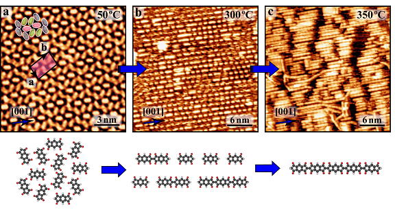
On-surface synthesis of aligned functional nanoribbons monitored by scanning tunneling microscopy and vibrational spectroscopy
N. Kalashnyk, K. Mouhat, J. Oh, J. Jung, Y. Xie, E. Salomon, T. Angot, F. Dumur, D. Gigmes, S. Clair, Nature Communications 8, 14735 (2017)
Growth of boronic acid based two-dimensional covalent networks on a metal surface in ultrahigh vacuum
S. Clair, M. Abel, L. Porte, Chemical Communications 50, 9627 (2014)
Electron spectroscopies like direct and inverse photoemission are powerful tools to explore the electronic properties of materials. One of the main aspects is their surface sensitivity making them particularly suited for the study of the interface between a thin organic film and an inorganic substrate. In the near ultra-violet range (UPS and IPES) the valence and conduction band are effectively probed. This can give valuable information about density of states of a thin film or the interface and on the adlayer/substrate energy level alignment. Such features are used in our group to study the interface bonding mechanisms and the charge injection barriers in organic/inorganic interfaces. Particularly, combining IPES and UPS the transport gap can be measured (see figure below, left panel).
XPS uses higher energy radiation and enables one to probe deeper electronic levels with elemental sensitivity. Moreover, since their binding energy depends on the valence charge distribution around an atom, energy shifts are used to probe the chemical environment of a given specie. Different oxidation states for –say- carbon within a given molecule can be detected by XPS, (see figure below, right panel) which can also shed light on the nature of the molecule-substrate interactions. Weaker interactions as intermolecular hydrogen bonds can also be detected.
Electron spectroscopies are performed in our group in two separate experimental setups: the IPES and the STM apparatus. In the first one, inverse (IPES) photoemission is available together with LEED, Auger, and standard preparation techniques. In the second UPS and XPS photoemission can be performed in parallel with in situ imaging by STM (LEED and preparation chambers also available). Moreover we regularly access to different synchrotron radiation facilities to perform high-resolution photoemission and photo-absorption experiments.
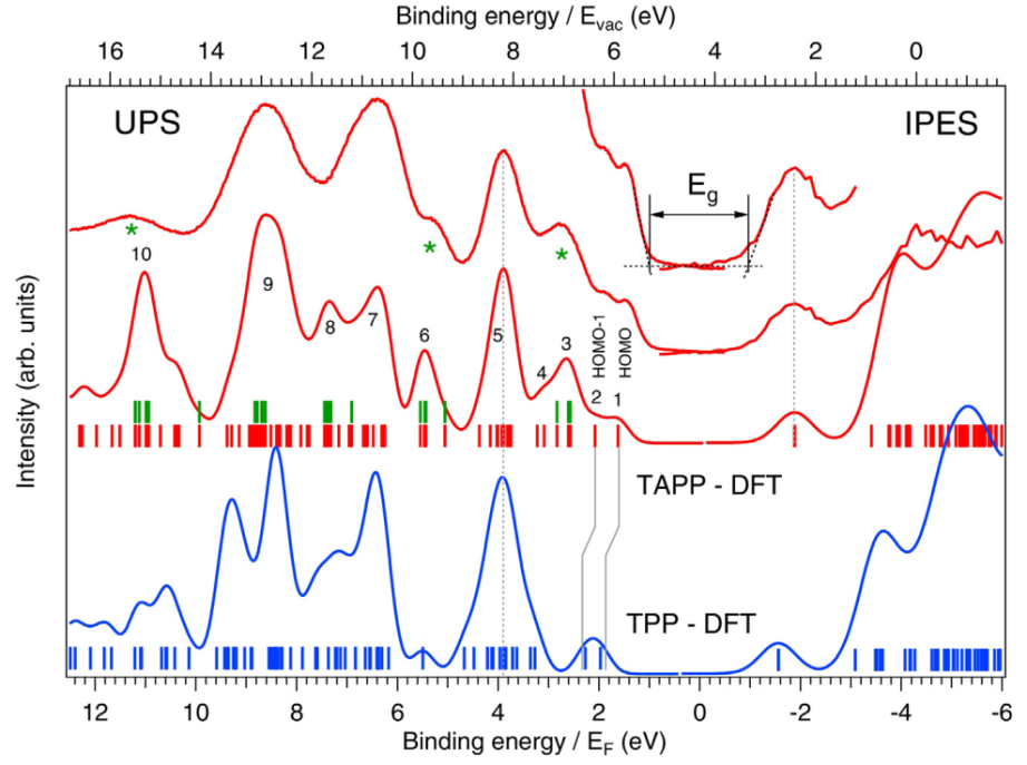
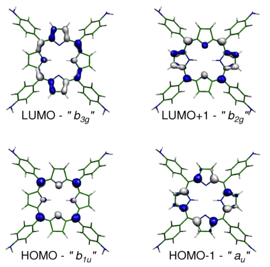
Direct and inverse photoemisison of the tetra(4-aminophenyl)porphyrin (upper spectrum). Comparison with DFT calculations (middle calculated spectrum) reveals that the presence of the two low-energy peaks in the filled states due to the lifting of the quasi-degeneracy of the HOMO and HOMO-1 in the non-substituted tetra-phenyl porphyrin (blue calculated spectrum). This is attributed to an increased HOMO orbital destabilization due to an enhanced electron-donor character of the phenyl substituents upon amino functionalization (see right panel). For more details see L. Giovanelli et al., J. Elec. Spectr. And Rel. Phen. 218, 40 (2017).
Probing the magnetic properties of 2D metal-organic systems by X-ray magnetic circular dichroism
π-conjugated macrocycles such as phthalocyanines and porphyrins hosting a single transition metal atom have shown great versatility in producing 2D magnetic arrays when adsorbed on well-ordered surfaces. This includes the possibility to modify the magnetic state of the metal atom through ferromagnetic or anti-ferromagnetic coupling to the substrate and by adsorption of smaller ligands (CO, O2). An alternative approach for the synthesis of magneto-organic nanostructures consists in manipulating the magnetic properties of transition metal atoms through selective bonding to functional ligands in surface-supported, self-assembled metal-organic networks. Thanks to the availability of synchrotron light sources and because of its capability of sensing the magnetic properties of a system in a element-selective way and down to the impurity level, X-ray magnetic circular dichroism (XMCD) is a preferred tool to study organic magnetic molecules. Through a close collaboration with the Magnetism (A. Savoyant) and Theory (R. Hayn) groups of IM2NP, we aim at investigating the magnetic properties of surface-supported 2D metal-containing organic systems using XMCD. In a first work we have revealed a ferromagnetic coupling between magnetic centers embedded in a metal-organic network on two different metal substrates. Angle and magnetic-field dependent measurements allowed to extract application-relevant parameters such as the magnetic coupling and single ion anisotropy.
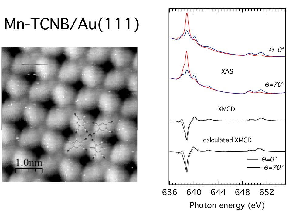
STM image of the Mn-TCNB metal-organic network on Au(111) and XAS spectra at different incident angle taken with opposite alignment between the circular polarization vector and applied magnetic field (6 T). The resulting XMCD spectra are modeled by multiplet calculations.
Molecules on semiconductors
Silicon Carbide (SiC) is a promising material for high-voltage, high-temperature and high-frequency electronic devices because of its wide bad-gap (~3eV), extreme hardness and thermal stability. Moreover, the diversity of its surface reconstructions triggers high interests in both the fundamental understanding of its surface electronic structure and possible applications. The interaction of organic molecules with SiC surfaces is of particular interest since it may lead to e.g. biosensors or optoelectronic devices. Besides, studying the electronic structure of organic molecules adsorbed on reconstructed semi-conducting surfaces may improve our understanding of organic thin film growth and molecular self-assembly mechanisms on semiconductor surfaces. In a recent study we have pursued a long-standing issue such as the binding of the ubiquitous C60 molecule on a Si-terminated surface, namely the 3x3-SiC(0001). High resolution synchrotron radiation XPS and UPS revealed that C60 is chemisorbed by orbital hybridization between the highest-occupied molecular orbital (HOMO) and the pz orbital of Si adatom at the apex of the tetramers.
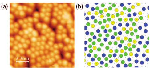
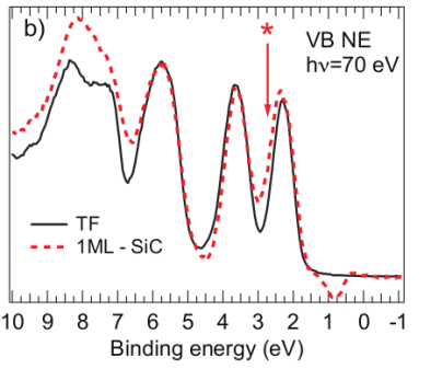
Left: experimental and simulations of sub-ML C60/3x3-SiC(0001). The abundance of energetically-closed adsorption sites (different colored disks representing C60 molecules) none of which holds a convenient conmensurability explains the lack of long-range order. Right: the UPS spectrum displays a high binding energy component suggesting an orbital hybridization to ensure the molecule-substrate bonding.
Selected publications:
Peculiar covalent bonding of C60/6H-SiC(0001)-(3×3) probed by photoelectron spectroscopy
F.C. Bocquet, L. Giovanelli, Y. Ksari, T. Ovramenko, A. J. Mayne, G. Dujardin, F. Spillebout, P. Sonnet, F. Bondino, E. Magnano and J.-M. Themlin, J. Phys.: Condens. Matter 30, 505002 (2018)
L. Giovanelli, H.-L. Lee, C. Lacaze-Dufaure, M. Koudia, S. Clair, Y.-P. Lin, Y. Ksari, J.-M. Themlin, M. Abel, A.A. Cafolla, J. Elec. Spectr. And Rel. Phen. 218, 40 (2017)
Nitrogen-doping processes of graphene by a versatile plasma-based method
Y.-P. Lin, Y. Ksari, J. Prakash, L. Giovanelli, J.-C. Valmalette, J.-M. Themlin, Carbon 73, 216 (2014)
Nitrogen-doping processes of graphene by a versatile plasma-based method
Y.-P. Lin, Y. Ksari, J. Prakash, L. Giovanelli, J.-C. Valmalette, J.-M. Themlin, Carbon 73, 216 (2014)
Since 2009, the experimental part of our research activities are focused on the structural, electronic and optical properties of organic molecules adsorbed on bulk dielectrics (ionic crystals) surfaces in the mono-layer regime. These are gathered into three topics:
- Structure and growth of supramolecular assemblies
- Optical properties of adsorbed organic layers by Differential Reflectance Spectroscopy
- On-surface polymerization processes
Our experimental tools are non-contact Atomic Force Microscopy (nc-AFM), Kelvin Probe Force Microscopy (KPFM), as well as Differential Reflectance Spectroscopy (DRS) in ultra-high vacuum (UHV).
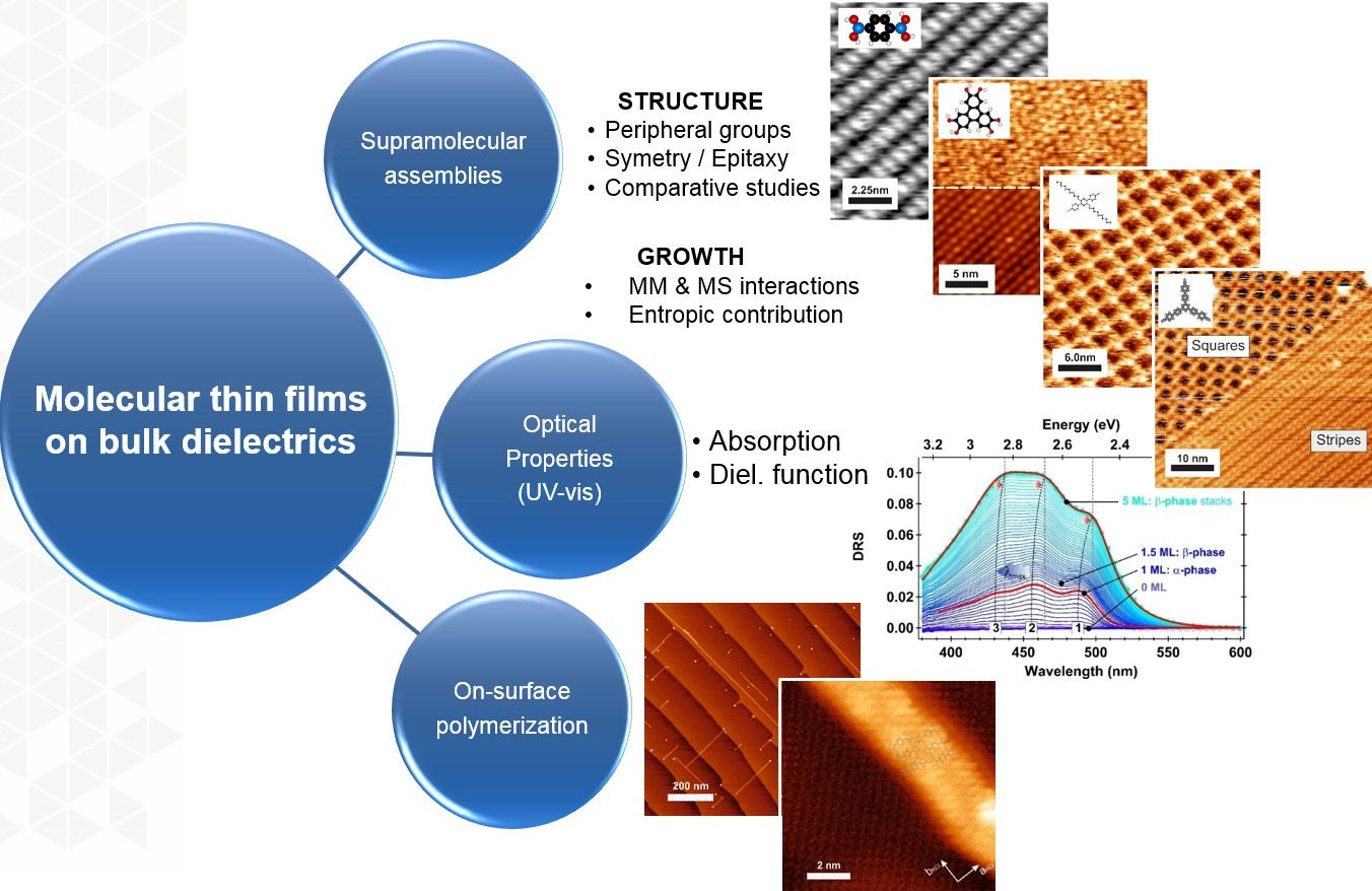
Figure : Overview of our experimental research activities
I.1- Structure and growth of supramolecular assemblies:
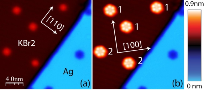
Our expertise is focused on the study of the structural properties of adsorbed organic molecules grown in the mono-layer regime at the surface of ionic crystals, such as alkali halides (NaCl, KCl, RbCl, KBr). At the surface, the molecules interact with each other without forming covalent bonds, but specific, long-range (~ a few angströms), hence weaker, intermolecular interactions forming so-called supramolecular assemblies.
The influence of:
- the molecule shape and symmetry
- the molecule’s peripheral groups
- the relative behavior upon adsorption of a given tecton on different substrates
- the molecule-molecule and molecule-substrate interactions
was investigated on a large set of molecules [1-4]. Our experimental results are systematically compared to Density Functional Theory-based calculations as-performed by colleagues from national or international institutions, which brings further insights from the understanding of the structures.
Thus, original types of growths were found out (line on line epitaxy). Polar peripheral groups and molecular entropy were also found to be key mechanisms to steer the ordered growth of the supramolecular assemblies.
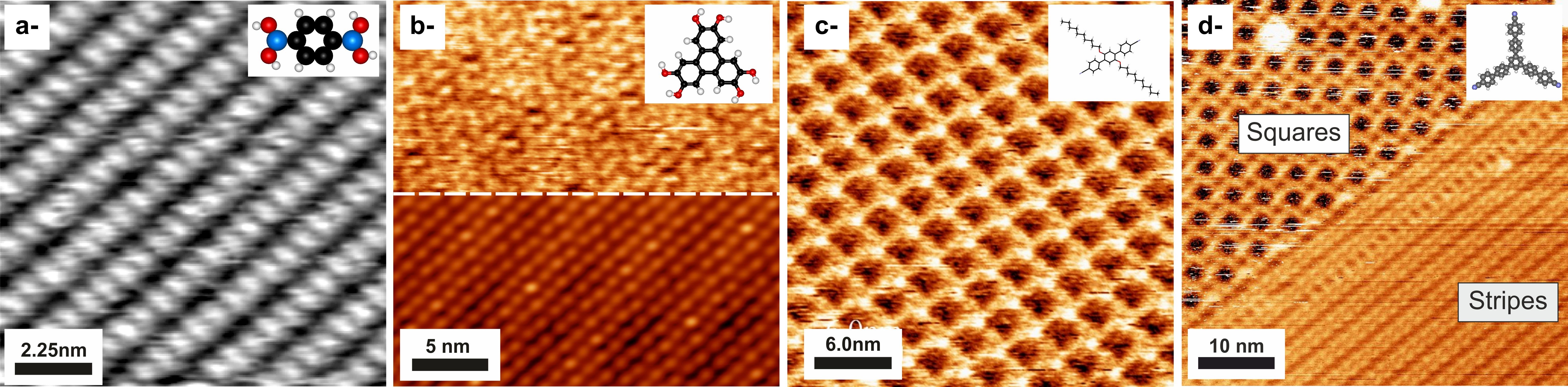
Figure : Examples of organic supramolecular assemblies on alkali halides substrates, as measured by nc-AFM. a- Boronic acid on KCl(001), after [1]. b- Hexa-hydroxy triphenylene on KCl(001), after [2]. c- 1,4-bis(cyanophenyl)-2,5-bis(decyloxy) benzene molecule on KCl(001), after [3]. d- 1,3,5-tri-(4-cyano-4,4-biphenyl) benzene molecule on KCl(001), after [4].
References :
[1] R. Pawlak et al., J. Phys. Chem. C 114, 9290 (2010)
[2] F. Bocquet et al., Phys. Rev. Lett. 108, 206103 (2012)
[3] A. Amrous et al., Adv. Mater. Interf., 1400414 (2014)
[4] J. Gaberle et al., J. Phys. Chem. C 121, 4393 (2017)
I.2- Optical properties of adsorbed organic layers by DRS:
Differential Reflectance Spectroscopy (DRS) is a real-time, UV-visible, spectroscopic method allowing for the measure of the reflectance changes of a surface upon adsorption of additional material. A DRS setup is adapted on our UHV setup (see "instrumental developments" section below). Hence, the DR spectra are recorded on materials grown in situ.
DRS is used to investigate the optical response of the organic adlayers adsorbed on insulating substrates such as alkali halide single crystals. The reflected specular light intensity is measured as a function of the wavelength, then normalized to the one of the bare substrate, which ultimately gives access to the absorption properties of the adsorbed adlayer.
The as-measured DR spectra are interpreted as functions of:
- the intrinsic molecular absorption (molar extinction coefficient)
- the geometric parameters of the deposit on the substrate (molecular unit cell, thickness, roughness, number of layers…)
The intrinsic molecular absorption are derived from regular spectroscopic methods (absorption / fluorescence) of the molecular tectons in solvants. The geometric parameters are derived from non-contact AFM experiments performed in the same UHV chamber. A typical set of DR spectra is shown in the fig. below, after [1].
An important piece of effort for the modelization of the DR spectra has been carried out that allows us to extract the dielectric function of each organic layer.
Further details on the experimental and theoretical aspects of our approach to DRS can be found here and here, respectively.
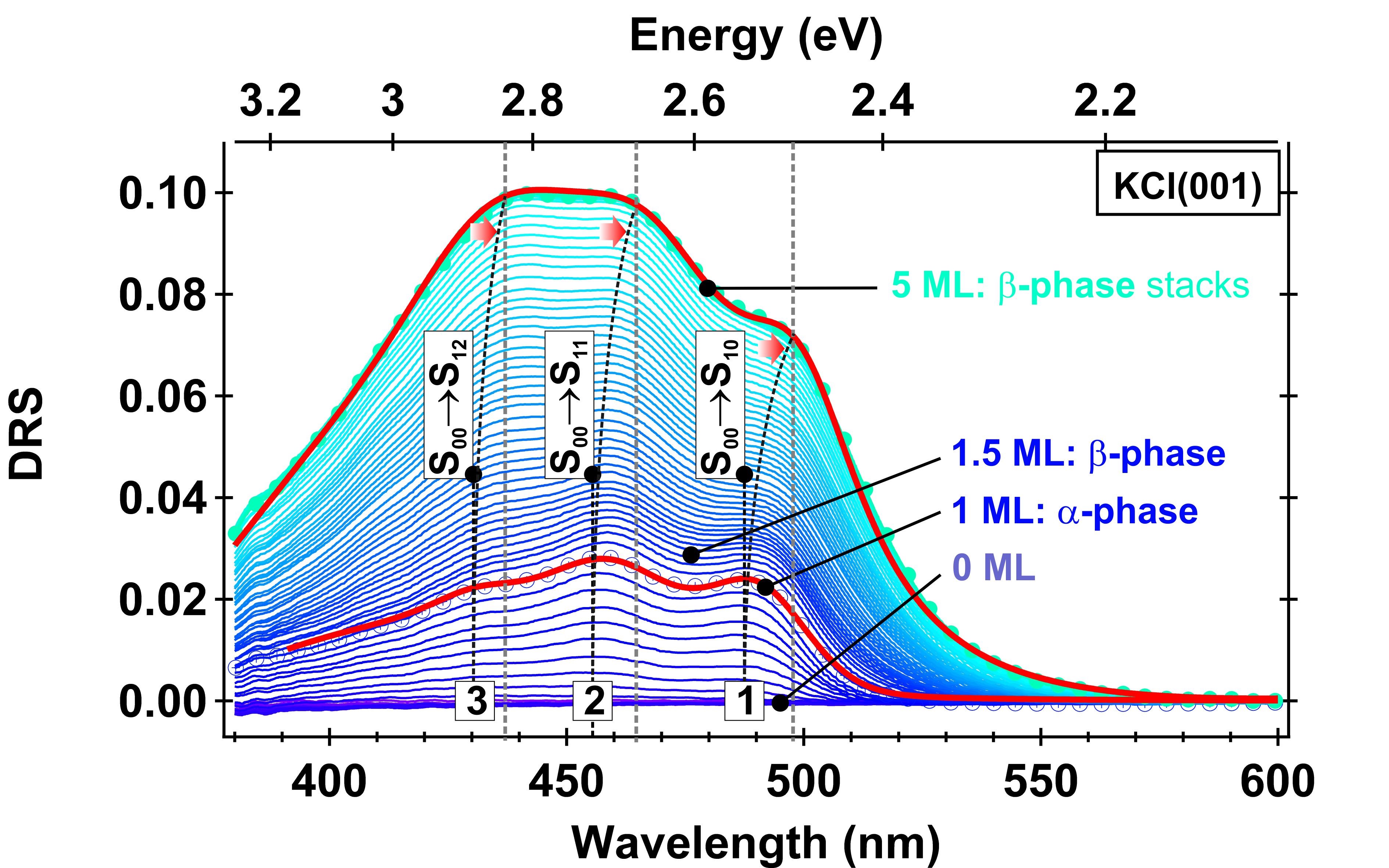
Figure : Reflected specular intensity (DRS signal) as a function of the wavelength measured during the growth of molecular layers of bis-pyrene molecules from 0 to 5ML (~ 10 nm) adsorbed on a KCl(001) substrate. Non-contact AFM structural data tell us the molecules form 2 phases (a-phase up to 1ML, b-phase above). Vibronic replicas are visible, which change as a function of the growth (1,2,3). Good-quality fitting (red curves) can only be achieved if a mix of a and b phases is considered (see [1]).
References :
[1] F.Bocquet et al. Phys. Rev. B 97, 235434, (2018).
I.3- On-surface polymerization processes:
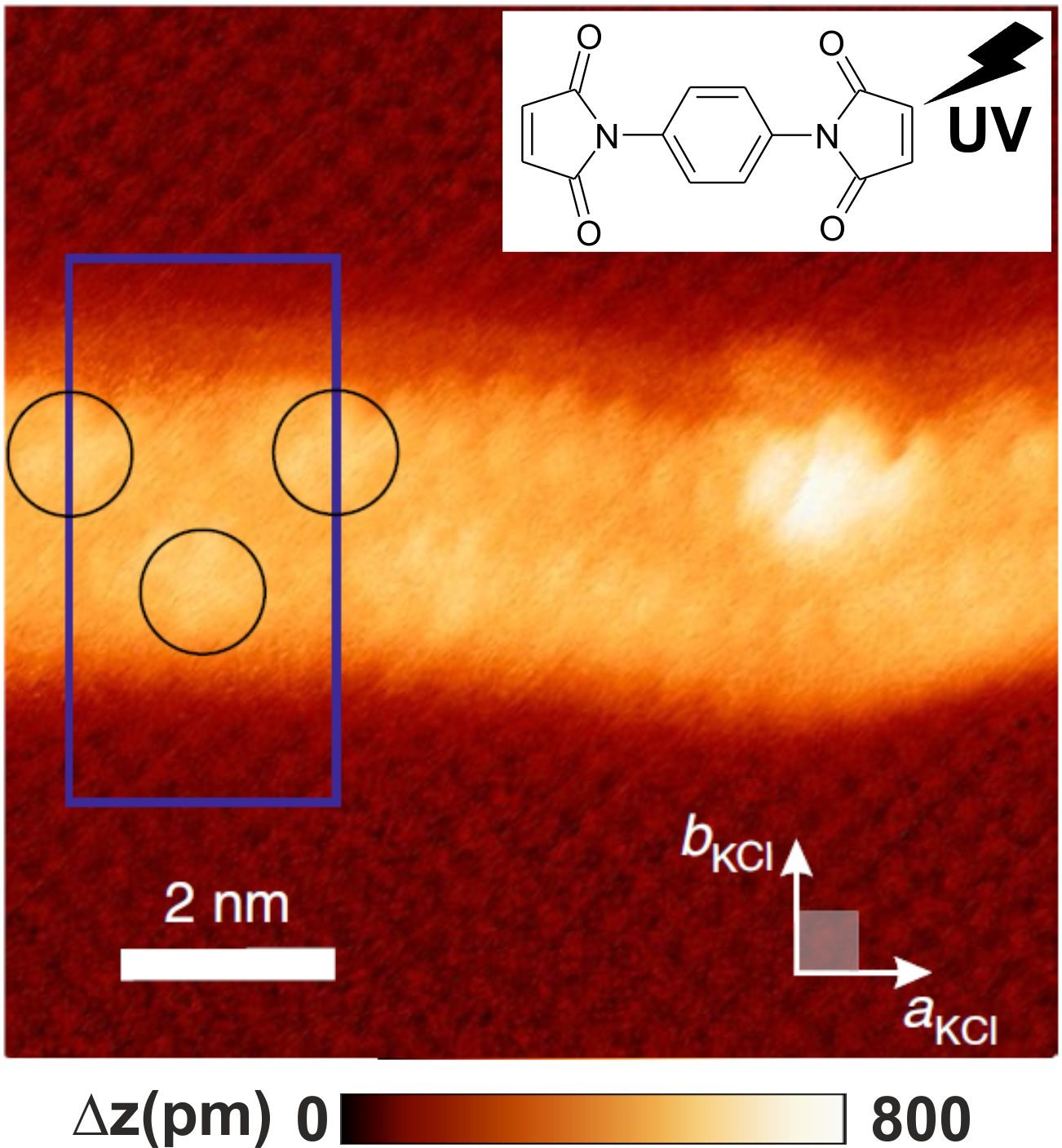
Figure : Dimaleimides molecules polymerized on a KCl(001) surface after UV irradiation. The nc-AFM image allows us to resolve the substrate down to the atomic scale as well as the polymer fiber with molecular resolution (after [1]).
References :
[1] F.Para et al. Nature Chemistry 10, pages1112–1117 (2018). DOI: 10.1038/s41557-018-0120-x
_________________________________________________________________________________
Our UHV setup is operational since December 2008. It consists of two inter-connected UHV chambers (base pressure 10-10 mbar), the “preparation” and the “analysis” chamber (P- and A-chamber, respectively).
The P chamber includes:
- two built-in molecular evaporators facing quartz micro-balances
- a heating stage allowing for the electron bombardment (up to 1500°C)
- an additional heating stage for temperatures up to 600°C
- a cleavage stage for cleaving in-situ the ionic crystals
- an ion gun
- the DRS setup (see "instrumental developments" section below).
The A-chamber includes:
- the VT-AFM from Omicron®. The instrument was optimized in several manners (see “instrumental developments” section below).
- a low current LEED-Auger Electrons spectroscopy setup from OCI MicroEngineering®
The driving electronics of the VT-AFM is a R9 from RHK®. It includes the PLLPro Control System for non-contact AFM and KPFM operations, a Piezo Motor Control unit for driving the macroscopic displacements of the sample, and the unit for driving the piezos. The interfacing between the VT-AFM and RHK's electronic was discussed in [1].
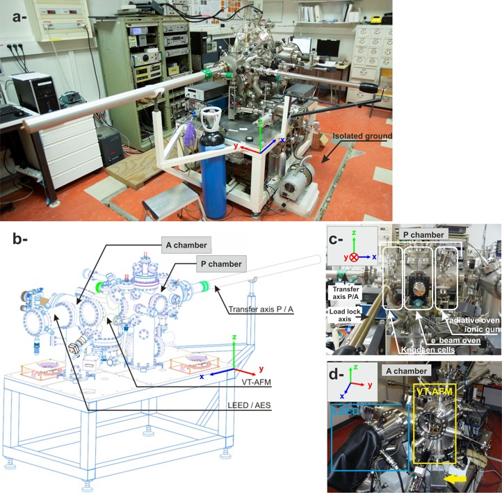
Figure : The UHV setup.
References :
[1] L.Nony et al. http://www.rhk-tech.com/wp-content/uploads/2016/02/R9_Omicron_ApplicationNote.pdf, RHK Technology Application Note (2015).
II.2- Instrumental developments:
II.2.a- Optimizations of the UHV VT-AFM:
The VT-AFM is a beam deflection-based instrument (probes=cantilevers) that was optimized to improve its nc-AFM/KPFM imaging performances. The AFM includes a two-stages preamplifier, the first stage being in UHV, beneath the 4-quadrants Photo Sensitive Detector (PSD). The second stage is located ex-situ and used for the conditioning of the I/V-converted PSD signals. It is referred to as the Mathbox and computes the vertical and lateral deflections of the cantilever.
A poster summarizing these optimizations can be found here.
The list of specifications of the instrument when used at room temperature is detailed hereafter:
- Light: Superlum diode @ 844nm (coherence length ~47nm); fiber output power: 4mW
- In-situ preamplifier (first stage): BDW = 3 MHz, I/V gain = 2200. Electrical consumption: 50 mW (per PSD channel). PSD reverse bias = -15V
- Mathbox (second stage): Calculation of the vertical and lateral deflection of the cantilever. Differential gain: x1.. x20. BDW = 1..5 MHz
- Noise floor on the cantilever oscillation signal: The noise floor of the instrument is 150 fm/ÖHz. Integration on the detection bandwidth (3 MHz) yields a rms noise on the oscillation amplitude of 300 pm.
- Oscillation amplitude: At 150 kHz (typical resonance frequencies of the cantilevers that are used), 1 nm oscillation amplitudes (peak-to-peak) provide enough stability for nc-AFM operation.
- Mechanical noise floor in the room: The AFM is located on a ground that is isolated by a trench from the rest of the building. The mechanical noise floor is 1 nm.s-2 for frequencies up to 10 Hz.
- Vertical noise (z channel, topography): The vertical noise is 5 pm typ. (see figure below).
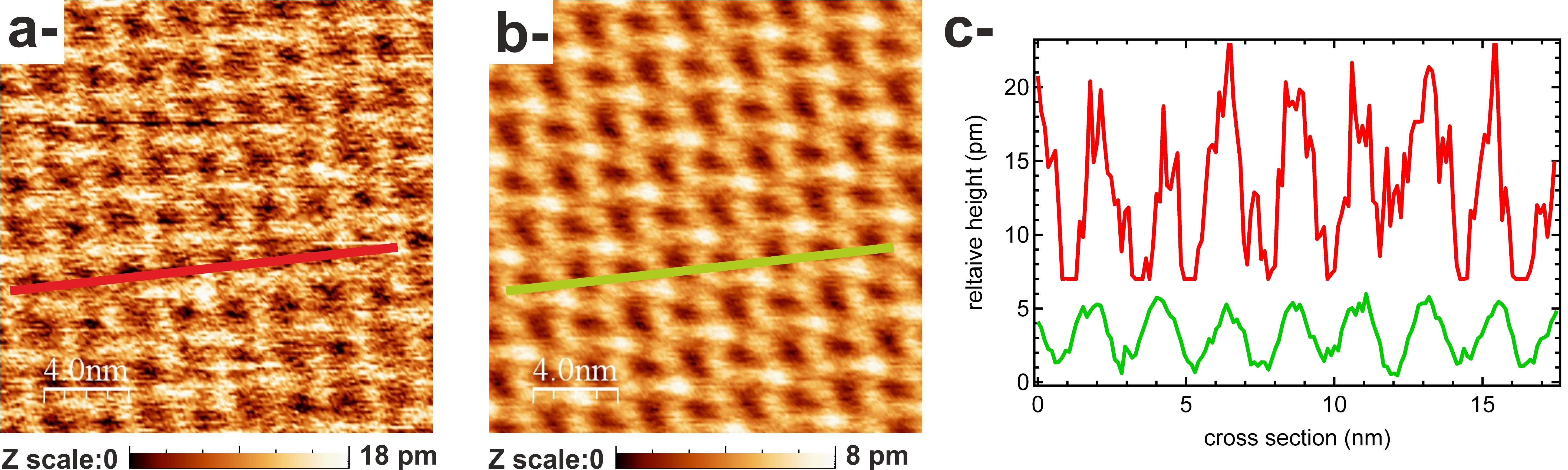
Figure : nc-AFM topographical images of 1,4-bis(cyanophenyl)-2,5-bis(decyloxy) benzene molecules on KCl(001). a- Raw data. b- Filtered data. c- Cross sections along red and green lines in a- and b- respectively showing the Z level of noise.
II.2.b- Differential reflectance spectroscopy:
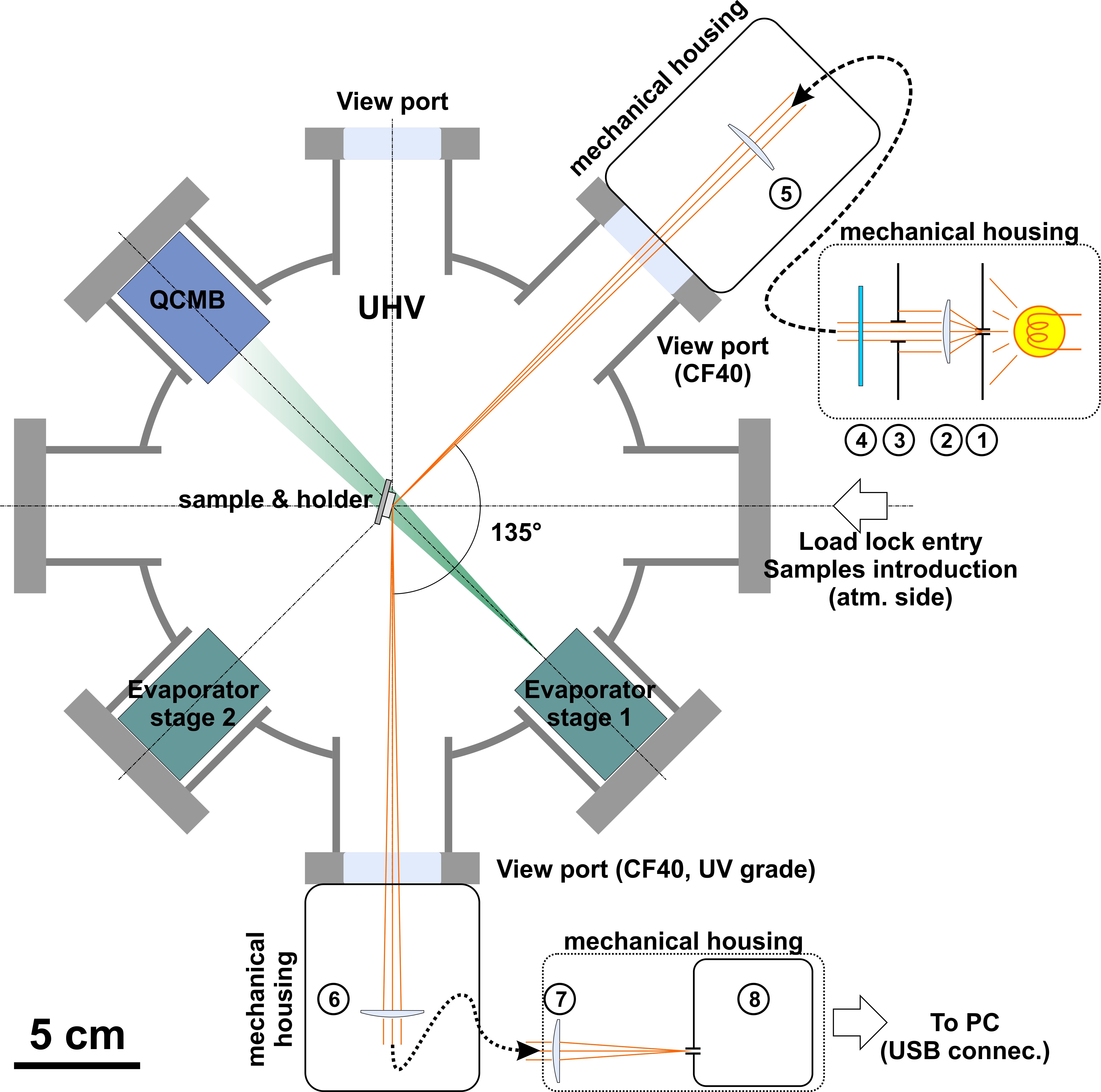
Figure: Implementation of the DRS setup on the P-chamber.
References :
[1] F.Bocquet et al. Phys. Rev. B 97, 235434, (2018).
II.2.c- Developments with quartz tuning forks-based nc-AFM probes:
Quartz tuning forks (QTF-) are commonly used as probes for combined nc-AFM/STM applications at low temperature. Nonetheless, they still remain controversial probes, as they can beget important interplay between frequency shift, damping and AC tunneling current (due to the oscillation of the tip) signals. The reasons for such a cross-talk remain under debate.
We have proposed an interpretation framework for that cross-talk [1]. It is inferred that AC tunneling current radiates an electromagnetic fields that penetrates the QTF's prong end and gets coupled to the piezoelectric tensor of the material. This unexpected field yields an additional deformation of the prong's end which is converted into motion, hence in additional, unexpected, oscillation of the QTF. This ultimately fakes both the information on the tip-surface distance, hence the frequency shift, but also the damping.
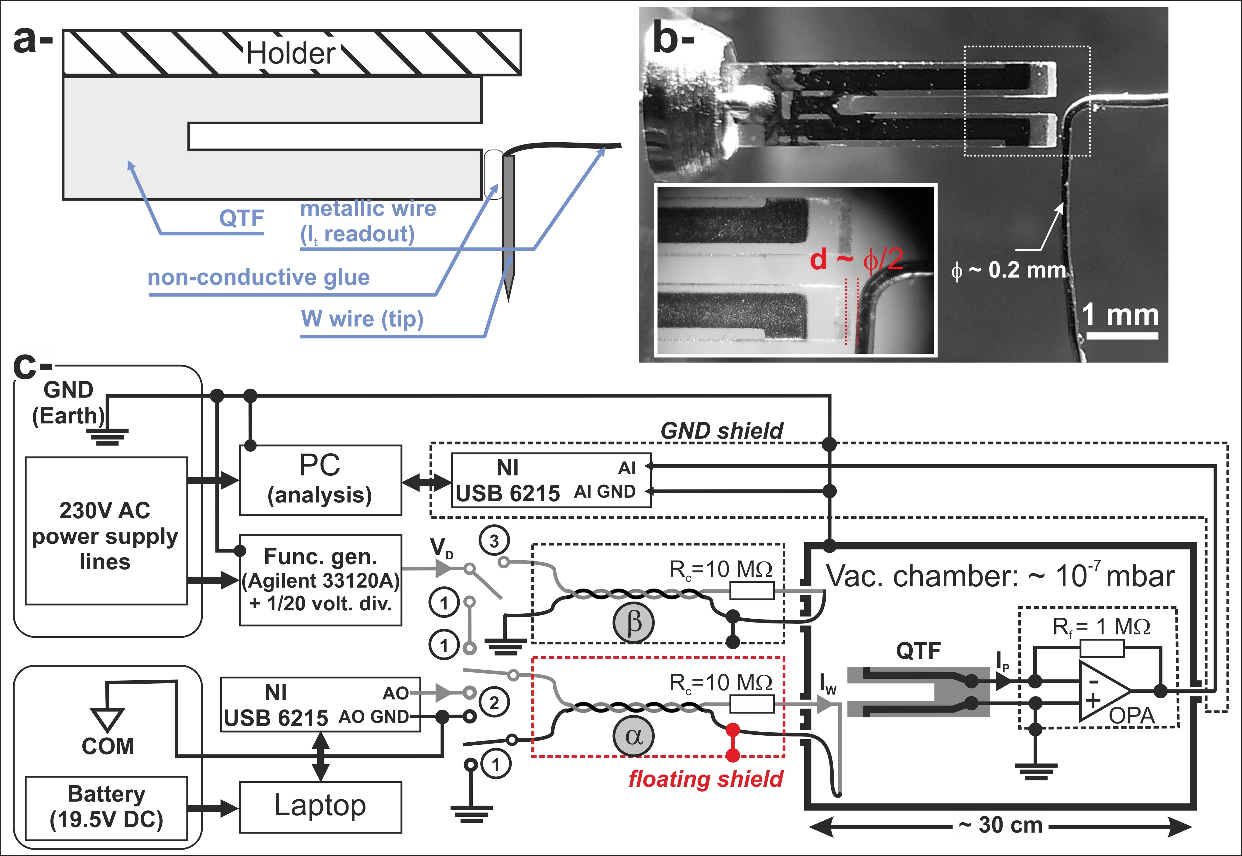
Figure: Scheme of the instrumental development on QTF
References :
[1] L.Nony et al. Phys. Rev. B 94, 115421 (2016).
_________________________________________________________________________________
III. Modelization:
Along with our experimental activities, an important part of our research was also focused on modelization and numerical developments in relation with the systems that were investigated experimentally.
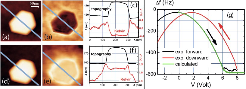
We have developed an analytical approach to the LCPD with the goal in mind to better understand the atomic-scale contrast observed while Kelvin Probe Force Microscopy measurements (KPFM) on KBr(001) [1]. The approach relies on the determination of the electrostatic force occurring between a metallic tip carrying a small metallic cluster in topmost position and the bulk ionic crystal below. The approach states that the ions at the surface undergo dynamic displacements (ionic polarization) under the influence of the inherent modulation of the bias voltage between the tip and the crystal that is required by the KPFM technique. The force, with a short-range nature, is site-dependent and has the lateral periodicity of the Madelung surface potential, i.e. the one of the underlying ionic lattice. It does not only scale quadratically with the applied bias voltage, but also linearly. The analytical approach to the KPFM method, i.e. actually the analytical expression of the DC potential that nullifies this force, namely the LCPD, shows that the latter force is responsible for the atomic-scale contrast in KPFM but that any quantitative connection to the physical observables such as the Madelung surface potential, or the local work function can be made owing to the convolution of the detected LCPD by the tip’s geometrical parameters [1,2].
References :
[1] F.Bocquet et al., Phys.Rev.B 24, 1791 (2008)
[2] L.Nony et al. Nanotechnology 20, 264014 (2009).
III.2- Simulating the nc-AFM/KPFM setup.
Following the analytical developments, we have implemented the KPFM operational mode within the core of an accurate numerical implementation of the nc-AFM setup, the so-called nc-AFM simulator [1]. With the fully numerical nc-AFM/KPFM setup, it is possible to simulate spectroscopic curves as well as topographical and LCPD images. In collaboration with Prof. Adam Foster from Tampere University (Finland), we have used the nc-AFM/KPFM simulator in combination with atomistic force fields computed between a tip with a realistic geometry and the NaCl(001) surface. This large computational effort strengthen most of the analytical results and led to the conclusion that the simultaneous occurrence of the atomic-scale topographical and KPFM contrast is possible (no experimental artifact, no cross coupling between channels), but that the latter relies on the dynamic polarization of the ions at the tip-surface interface. This makes any quantitative measurement of the Madelung surface potential possible [2,3]. However, the “chemical” periodicity remains preserved. Further details can be found here.
References :
[1] L.Nony et al., Phys.Rev.B 74, 235439 (2006)
[2] L.Nony et al., Phys.Rev.Lett. 103, 036802 (2009).
[3] L.Nony et al. Chapter in the book «Kelvin Probe Force Microscopy», (Eds. Sascha Sadewasser & Thilo Glatzel), Springer-Verlag Berlin Heidelberg (2011), DOI 10.1007/978-3-642-22566-6
III.3- Methodology for fitting the DR spectra
References :
[1] F.Bocquet et al. Phys. Rev. B 97, 235434, (2018).
Raman spectroscopy is a vibrational spectroscopy based on inelastic light scattering. As such, it is a powerful analysis tool in the field of materials. Nevertheless classical Raman spectroscopy is limited by its very low cross section. Since 10 years, our team is developing a research activity based on Surface Enhanced Raman Spectroscopy (SERS). This technique is based on plasmonic nano-antenna, usually gold nanoparticles. The Raman signal is strongly enhanced by those antennas, increasing the final cross section of the Raman process. It is thus possible to detect molecules in very low concentration. An example of such nano-antenna can be seen in the figure below.
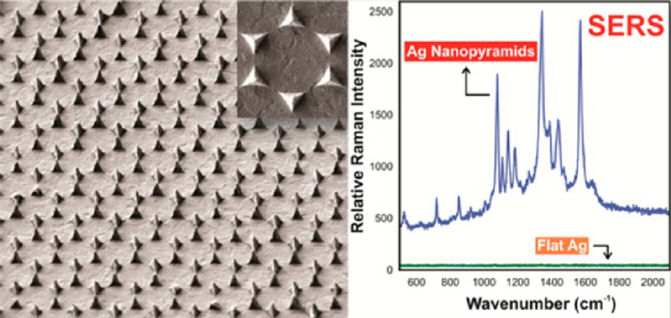
Figure: An exemple of 3D plamsonic nano-antennas for SERS. This work has been performed in collaboration with the University of WESTERN Ontario
In addition to SERS, our team is developing an apertureless scanning optical microscope based on a single nano-antenna fixed at the APEX of a scanning probe. This approach is named Tip Enhanced Raman Spectroscopy (TERS). It has two major advantages: a high sensitivity associated to a high spatial resolution (typically a few nanometers).
All those works are performed in collaboration with several laboratories (UWO and INRS, Canada and PIIM, France).
Selected publications:
J. Plathier, A. Merlen, A. Pignolet, A. Ruediger, J Raman Spectrosc. 2017; 48 (12), 1863-1870.
A. Merlen, C. Pardanaud, S. Coussan, C. Panagiotopoulos, O. Grauby, Carmen M. Ruiz, J Raman Spectrosc. 2018 ;49 (7), 1184-1189.
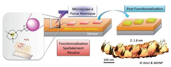
In catalytic scanning probe lithography (cSPL), the tip of an AFM is modified to accommodate a catalyst, usually a metal deposited as a thin film or in nanoparticule form. Part of the reactants is provided on a surface in the form of a self-assembled monolayer (SAM) bearing reactive endgroups, and the remaining reactants are solvated in the surrounding liquid. A chemical coupling reaction is initiated locally by mechanical application of the catalytic tip and various chemical compounds can be grafted selectively, with a spatial resolution in the order of a few tens of nm. The technique can be extended to the use of homogeneous catalyst immobilized onto the tip upon modification with an appropriate ligand. The use of a homogeneous catalyst opens in principle the way to a large variety of chemical reactions. It was shown that the catalytic activity of the tip-supported catalyst was barely affected during the reaction process, and large areas could be covalently modified without significant loss of the reactivity.
This thematic is developed in collaboration with Jean-Luc Parrain and Olivier Chuzel from iSm2 laboratory.
Selected publications:
J. Botton, K. Gratzer, C. François, V. Mesquita, L. Patrone, T.S. Balaban, S. Clair, J.-L. Parrain, O. Chuzel, Chemical Science 9, 4280 (2018)
V. Mesquita, J. Botton, D.A. Valyaev, C. François, L. Patrone, T.S. Balaban, M. Abel, J.-L. Parrain, O. Chuzel, S. Clair, Langmuir 32, 4034 (2016)
D.A. Valyaev, S. Clair, L. Patrone, M. Abel, L. Porte, O. Chuzel, J.-L. Parrain, Chemical Science 4, 2815 (2013)
|
Date |
Project name |
Collaborators |
|
2024-2028 ANR PRC |
PESOS: Imaging the Photo-Excited Electronic States at the Molecular Scale |
Institut Néel B. Grévin) |
|
2023-2025 AMIDEX |
ATOPRINT: Atomically-printed 3-dimensional molecular assembly |
ICR (D. Gigmes) |
|
2022-2026 ANR PRC |
Light4Net: Photo-Induced On-Surface Synthesis to Elaborate Highly-Ordered Covalent Structures on Insulating Substrates |
FEMTO-ST (F. Cherioux) |
|
2022-2026 ANR PRC |
GANESH: Graphene Nanomesh |
CEA-IRAMIS (S. Campidelli) LUMIN-ENS (JS. Lauret) CEA-SPEC (S. Latil) |
|
2021-2025 ANR PRC |
CROSS: Controlled Reactivity of Sulfoxides on Insulating Surfaces |
CEMES (C. Kammerer) LHFA (D. Madec) |
|
2017-2022 ANR PRC |
DUALITY: Surface-directed Elaboration of Two-dimensional Nanoporous Covalent Organic Frameworks |
ICR (F. Dumur) PIIM (E. Salomon) |
|
2018-2020 AMIDEX |
MATMOL: Acquisition d’un système combiné AFM/STM ultra-vide basse température pour l’étude de MATériaux MOLéculaires nanostructurés avec résolution intramoléculaire |
ICR (D. Gigmes) |
|
2017-2020 Région PACA |
MOLOS: Acquisition of a Low-Temperature AFM/STM for the study of one- and two-dimensional organic systems with sub-nanometer resolution. (Acronym MOLOS, MOLecules On Surfaces) |
ICR (D. Gigmes) |
|
2016-2020 ANR PRCI |
PHOTONET: On-surface synthesis of covalent networks with integrated optical functions |
ISM2 (JL. Parrain) RIKEN (Y. Kim) |
|
2013-2016 AMIDEX |
REBICOF: Two-dimensional functionalized covalent organic frameworks |
ICR (D. Gigmes) |
|
2013-2016 ANR PRC |
CASPARES: CAtalysis SPAtially REsolved on a Surface |
ISM2 (JL. Parrain) |
|
2010-2013 ANR JCJC |
COVANET: Functionalized covalent 2D networks for immobilization of transition metal atoms |
ICR (D. Gigmes) |
Mots clefs
Surfaces and interfaces
Scanning Probe Microscopy
Photoelectron Spectroscopy
Raman Spectroscopy
Scanning Probe Microscopy
Photoelectron Spectroscopy
Raman Spectroscopy
Collaborations
![]() The Nanostructuration Team is part of the inter-laboratory team Nano-Mat-Mol with CINaM laboratory.
The Nanostructuration Team is part of the inter-laboratory team Nano-Mat-Mol with CINaM laboratory.


![]()
Actualités
Séminaire 23/09/19 - David Martrou - Controlling the electric charge of gold nanoplatelets on an insulator by field emission nc-AFM
Salle des séminaires de l'Im2np, campus de Saint-Jérôme, aile 1, niveau 6 service 161
-
Séminaire Maria Dekermenjian - 16 Mai 2019 - Effet de la spectroscopie Raman exaltée par effet de pointe (TERS) sur les modes Raman du premier ordre
Amphi Y1-012, campus de la Garde, Université de Toulon
-
Séminaire 03/04/19 - Sébastien Gauthier - CEMES, Toulouse
Salle des séminaires de l'Im2np, campus de Saint-Jérôme, aile 1, niveau 6 service 161
-

Séminaire Nataliya Kalashnyk - 26 Février 2019 - GeePs, Gif sur Yvette
Salle des séminaires de l'Im2np, campus de Saint-Jérôme, aile 1, niveau 6 service 161
-

Séminaire Azza Hadj Youssef - 14 Février 2019 - Manifestation de l'effet flexoéléctrique dans les couches minces de titanate de strontium.
Salle Y1-012, Campus de la Garde, Université de Toulon
-
Séminaire Hocine Khemliche - 5 décembre 2018- Modes d’organisation d’interfaces organique/inorganique révélés en temps réel par diffraction d’atomes rapides en incidence rasante.
Salle des séminaires de l'Im2np, campus de Saint-Jérôme, aile 1, niveau 6 service 161
-
Franck BOCQUET
permanent

Sylvain CLAIR
Directeur de recherche CNRS
Virginie GADENNE
Non permanent
Luca GIOVANELLI
permanent
Younal KSARI
Maître de conférences

Christian LOPPACHER VOIROL
permanent
Jean-Marc THEMLIN
permanent
Héla MREZGUIA
Non permanent
Laurent NONY
Maître de conférences
Franck PARA
Ingénieur de recherche - PhD
Lionel PATRONE
permanent
Publications
| Publications |
|---|